I’ve had a few requests to put together a guide on my PCB bubble wrapping technique. There’s a lot of text here because I wanted to provide insights into why I chose this method and do it the way that I do. But if you just want to know how to wrap, scroll down and follow the pictures. I tried to make it good enough that you could follow this guide without reading any text…
The Problem
I’ve got a lot of arcade PCBs, over 500 at last count. Storage has always been an issue. How do you keep them safe and dry, dust free, and static free while also keeping them compact and a solution that works for tiny boards like a Cave CV1K all the way up to an old SNK Triple Z80 3-board stack, and something that’s not going to cause me to go broke implementing it x500?
More than just storage on a shelf, securing a board for shipping can be an issue too, you want something that protects it on all sides but doesn’t put pressure on weak components like large capacitors or hard to replace custom modules that could snap if over stressed. And of course you want it to survive the trip while assuming that the carrier is going to handle your precious package like a football.
Other Solutions
I didn’t like any of my current solutions so I set out to find something better. I’ve tried many solutions suggested online, and been disappointed by, or take issue with most of them. I’ve seen custom acrylic cases, fancy anti-static boxes, and while those certainly make ease of access to the PCB great they’re incredibly bulky and expensive (particularly at scale), and they really only work for a limited size-range or sub-set of PCBs. I also feel strongly that these solutions aren’t actually that great as acrylic cases often put pressure on the corners of the PCB and anti-static boxes put pressure on all those fragile components, even with customizing the foam. Of course they’re much better than the options at the other end of the spectrum of bubble bags or non-bubble anti-static bags, or just empty USPS boxes which are all only weak partial solutions. Heck, even most original kit boxes do a poor job at protecting the PCBs as they were typically designed for one-time shipping and then getting thrown away.
Bubble Wrap
One thing I’ve always appreciated is that many of the Japanese PCB shops and proxy services did excellent work safely packing their boards. One company in particular, Try Amusement, had a sort of origami way of folding bubble wrap around their PCBs that looked and worked great.
What makes this solution great is that Bubble wrap is fairly inexpensive, because it comes on a roll it works for nearly every shape and size PCB. If you need more protection you can just add more layers and if you fold and cut it correctly it doesn’t take up any more space than it needs to. For oddly shaped PCBs with some bubble wrap and tape you can also create custom shaped pads that fill gaps and add protection in the right places. Of course you can also get it in anti-static variants which is important.
The Goals:
- I wanted to have a wrap that protected all faces and edges of the PCB with a similar number of layers;
- I wanted to to be even and flat and uniform, no weird bulky bulges on one side or unprotected corners.
- I wanted it to be re-usable so if I unwrapped a PCB I could do so without destroying the wrap and re-use it once I wanted to put the PCB back into storage.
- I wanted it to work with a single piece of tape; just enough to keep it from unraveling, this would also be key to the re-usability
- I wanted it to be as compact as possible. lots of PCBs takes up lots of space so every mm of unnecessary thickness on the PCB is getting multiplied and eating away at storage capacity.
Development
Try’s folding method seemed pretty good but wasn’t quite perfect. I did find a guide online for a folding method that was similar to Try’s. I followed this guide and it worked pretty well, but I also realized that it could be improved. Mostly it required several pieces of tape to secure the final wrap. I saw a few ways in which the folds and cuts could be modified to make a better solution. I actually had 4 or 5 versions of my solution before I landed on the one I now use for all of my PCBs. I think the solution I landed on meets all of my goals. so here it is…
twisted’s PCB Bubble Wrapping Method
What you’ll need:
- The PCB you want to wrap
- A smooth flat surface to work on
- A large Roll of 24in wide Anti-Static Bubble Wrap with 3/16th size bubbles. Opt for higher strength bubble wrap and don’t bother with perforations for easy tear away (you lose the occasional row of bubbles to this and it rarely lines up to where you need to make a cut. I buy large industrial sized rolls from ULine, I would love to find some “double walled” bubble wrap that has the flat wall on both sides sandwiching the bubbles, but I’ve yet to find a source for this that is also both anti-static and 24in wide. (if you know of one, let me know!)
- A good Pair of Scissors
- Tape, ideally Japanese Polyethylene cloth tape (or Japanese Happy Tape as I like to call it because it’s literally a joy to use and always wrapping something that makes me happy). Alternatively you can use clear packing tape. Polyethylene cloth tape is designed to be re-usable, and I have a method to make clear packing tape reusable-ish.
- [Optional] Labels – if you want to be fancy you can print and cut them out, or just use a sharpie to write it out. in either case I like to secure them with a piece of clear packing tape over the entire label
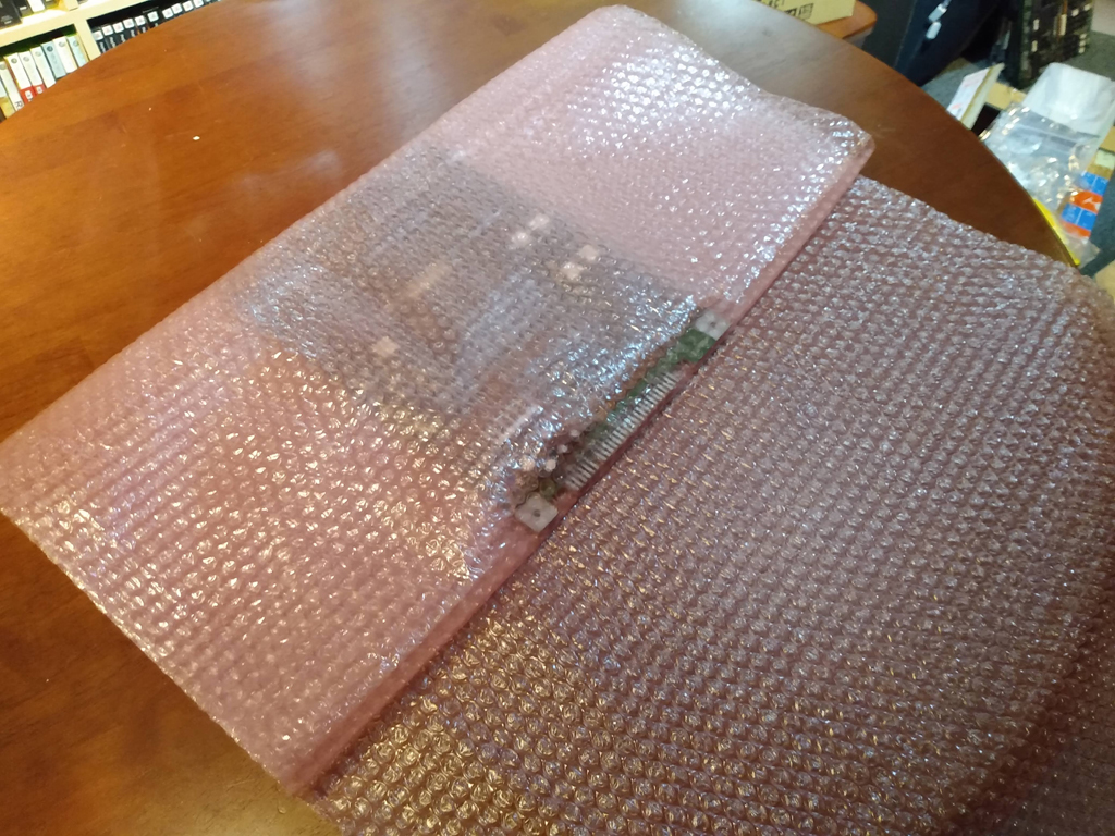
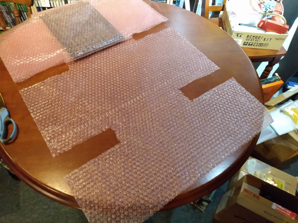
Step 1 – Lining it up
- Unroll some of your bubble wrap onto your work surface bubble side up.
- Place the PCB in the center, parts side up with the JAMMA edge pointing towards the roll
- make sure it’s centered and squared. I like to look at the back edge of the PCB and ensure it’s lined up with a row of bubbles.
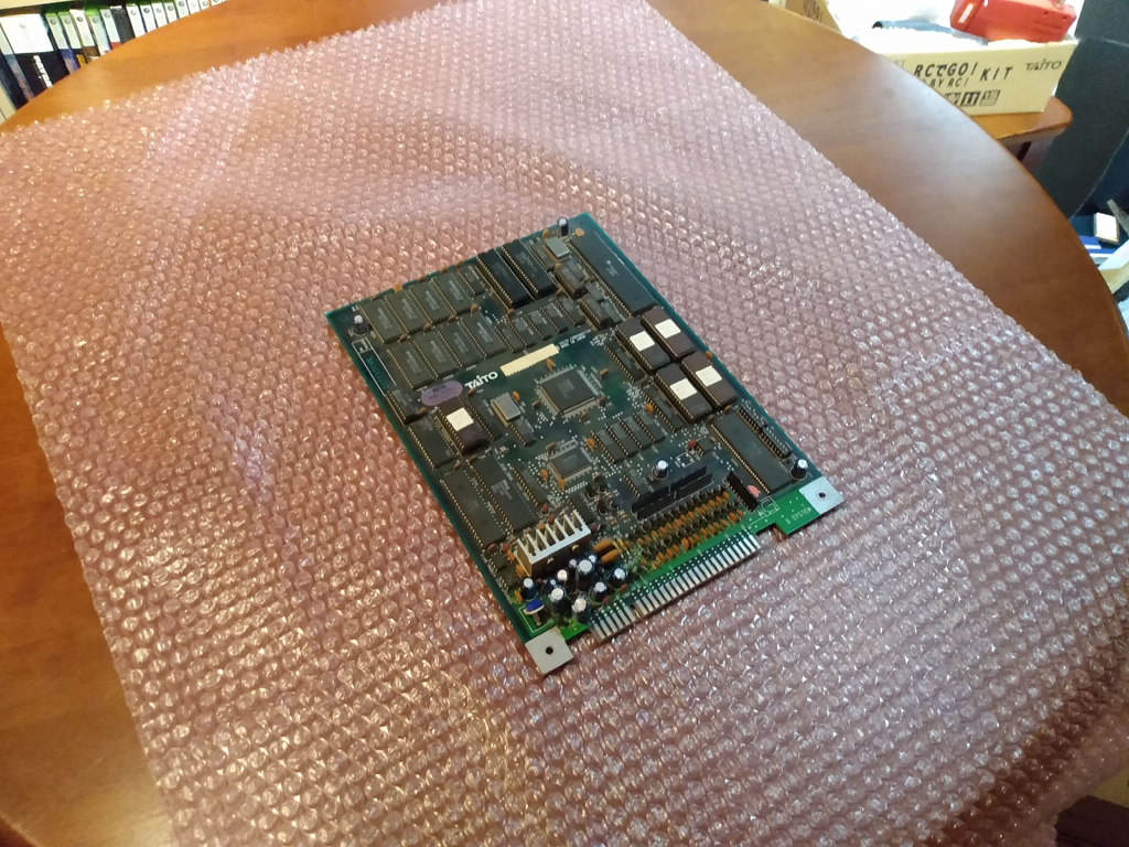
- Fold the bubble wrap over the back edge so that it covers the top of the PCB. Again you’ll want to make sure the alignment is as good as you can get it. You want to make sure that the flap is NOT longer than the PCB.
Pro-Tip: it’s actually better to be too short than too long here, sometimes if I have a PCB with a particularly obnoxious heat sync near the front edge I’ll intentionally fold this flap short so that it doesn’t’ cover the heat sync.
If you wanted extra protection of the JAMMA edge you might opt to go long enough to wrap around the front edge a bit. but it’s one of those things where you either want it shorter than the PCB or several cm longer than the PCB to make a secure wrap. anything in-between wont work. I’d advise trying it the way I have it shown to start, and then experiment with your own variations if you like.
Step 2 – Flipping it
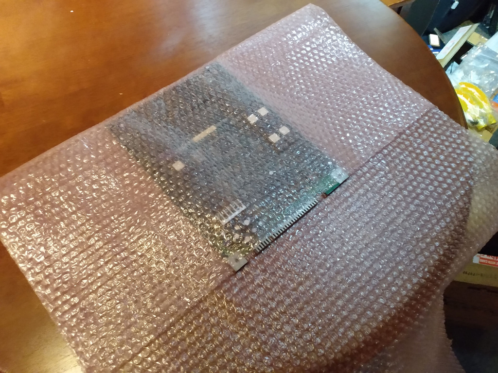
- Once you have the PCB aligned and and covered by the first flap, keep the Bubble wrap aligned, taught, and flat and flip the board toward the roll
- keep it aligned, taught, and flat and flip it a second time
- at this point your PCB should be back in it’s original, upright, position and have 2 layers top and bottom. Take a moment to ensure that all of the edges of the bubble wrap are aligned and that all of the bubble wrap is taught and flat up against the PCB (in case you haven’t realized, this is important)
Pro-Tip: If you want more protection, flip it two more times at this step. You’ll find that even with the flips we’ve done up to this point though by the end of the process we’ll end up with 4 layers on each face which should be more than enough. I’d encourage you to try the process first as I’ve presented and then experiment with your own variations after.
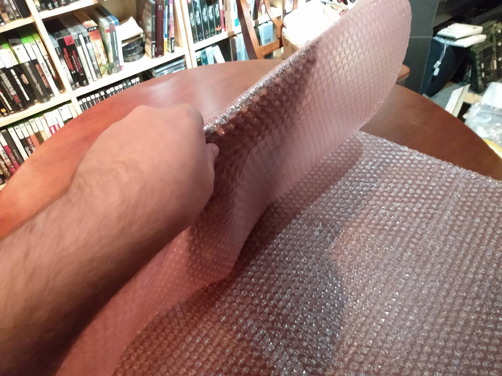
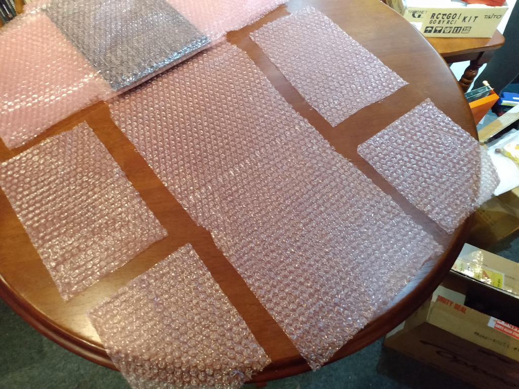
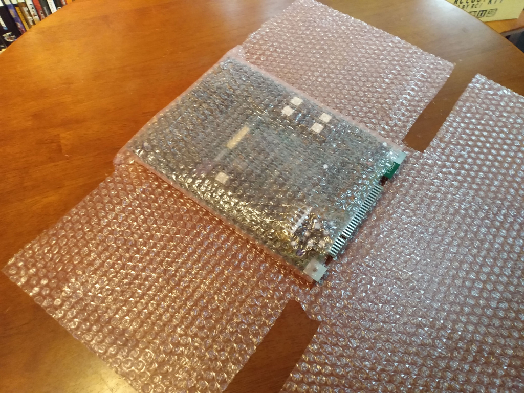
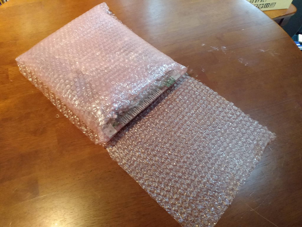
Step 3 – Cuts
- Cut off the roll creating a flap that’s long enough to end about mid way along the PCB. the precise length isn’t critical. It’s actually better to be a little too long here than too short as this flap will actually get slightly shorter once we’re done.
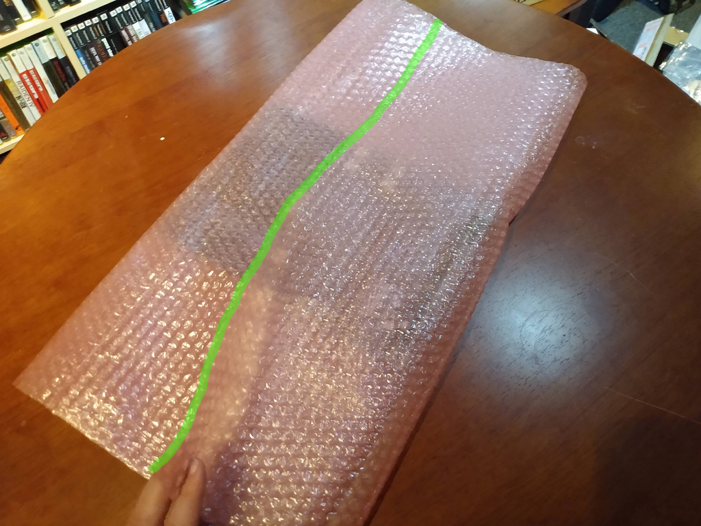
- With your scissors perpendicular to your wrapped PCB cut out one of the corners, you should be cutting out about 1cm (~0.5in) in from the corner and stop about 1cm (~0.5in) before you reach the PCB. The result here should be the removal of some small ~2cm (~1in) wide strips of bubble wrap. [DO NOT be tempted to turn the scissors parallel with the board and make a single slit cut without removing any material, as you’ll end up with bulk later. Similarly if you cut too close to the PCB it can leave your PCB’s corners with less protection.]
- Repeat this for the other 3 corners
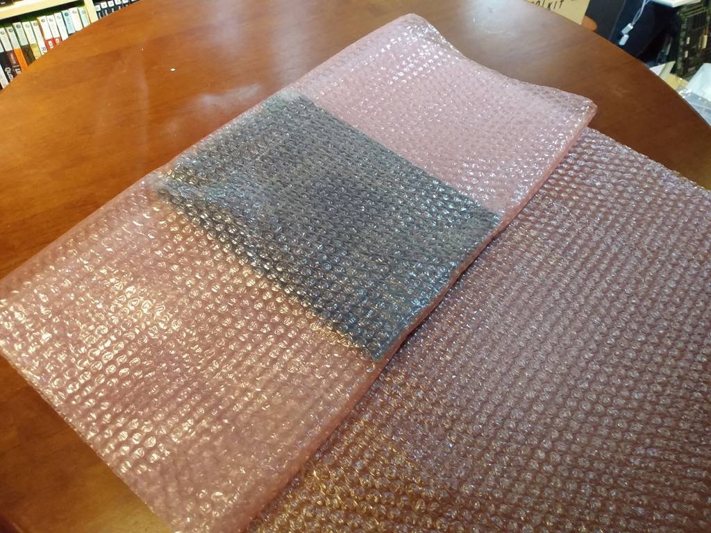
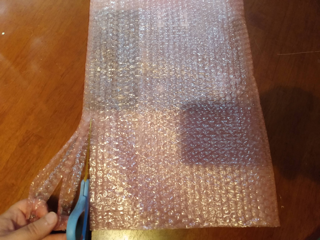
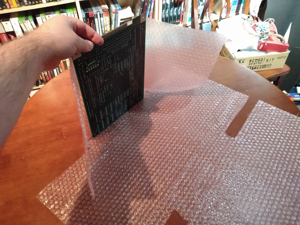
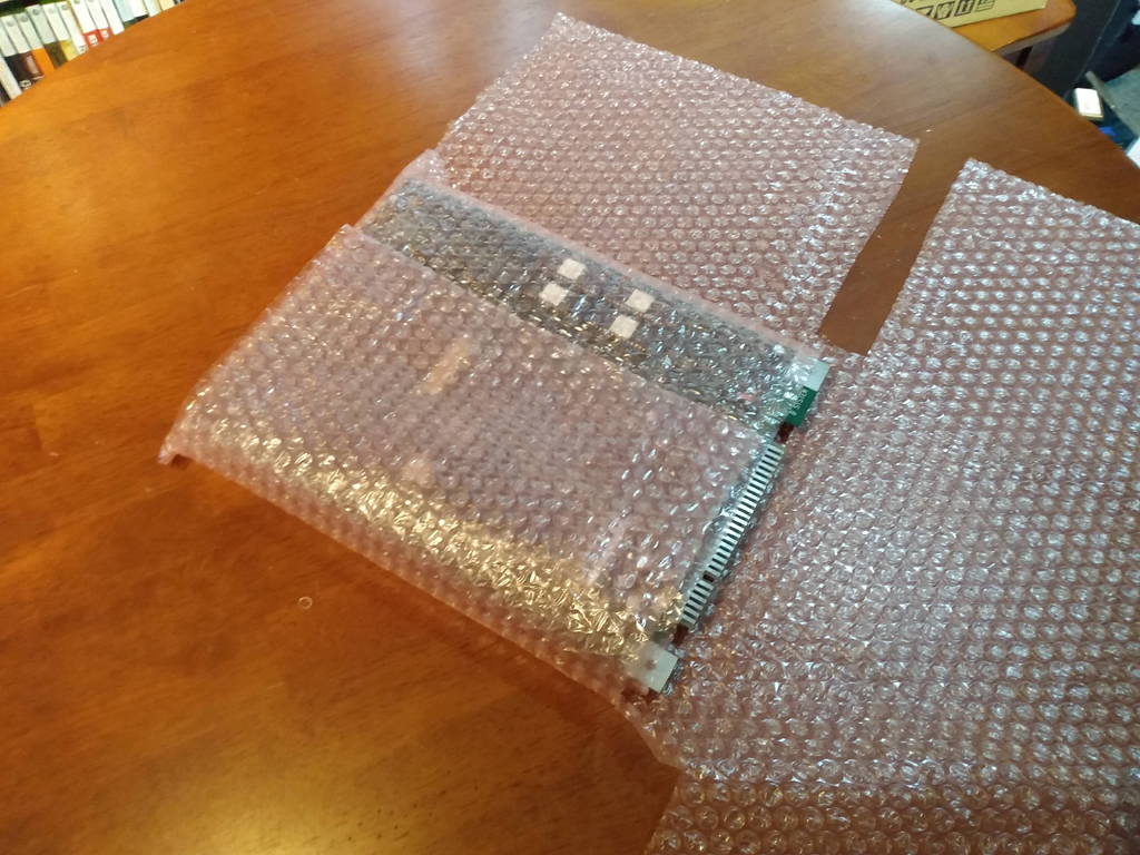
- Unfold the flap and then flip the board one time to unravel it as shown below.
- You’ll see what look like wings extending beyond the center section, you’ll want to cut-off these 4 wings as shown below. [Again, don’t be tempted to leave these on, this is critical to making this wrap re-usable and able to be secured with a single piece of tape.]
- The piece you’ve cut off can be discarded. though sometimes I do save some of the wings to make extra padding for PCBs that need extra protection near delicate parts.
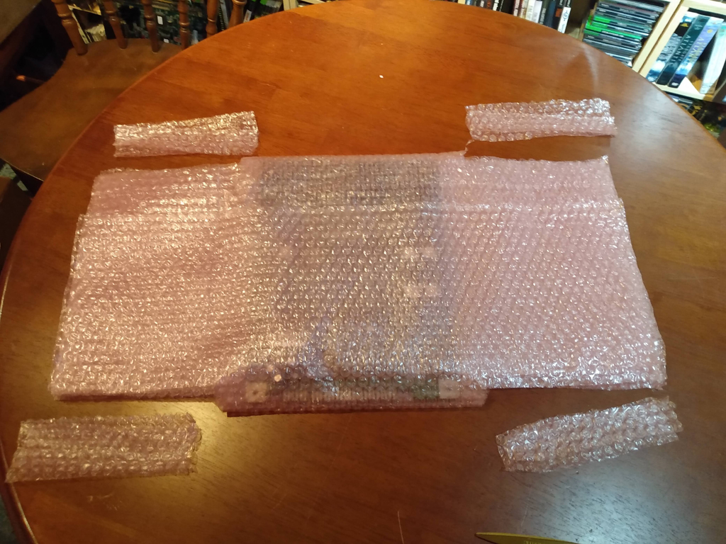
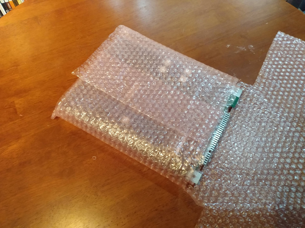
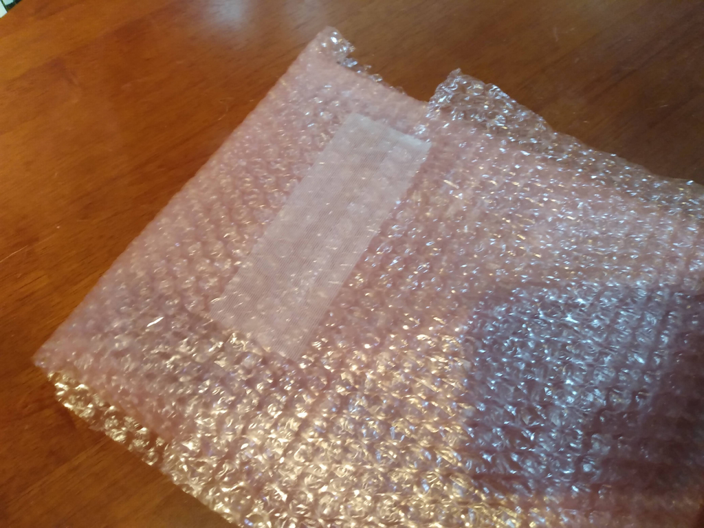
Step 4 – Wrapping
- Continue to flip and unravel the bubble wrap from your PCB until the bottom of your PCB is uncovered as shown below
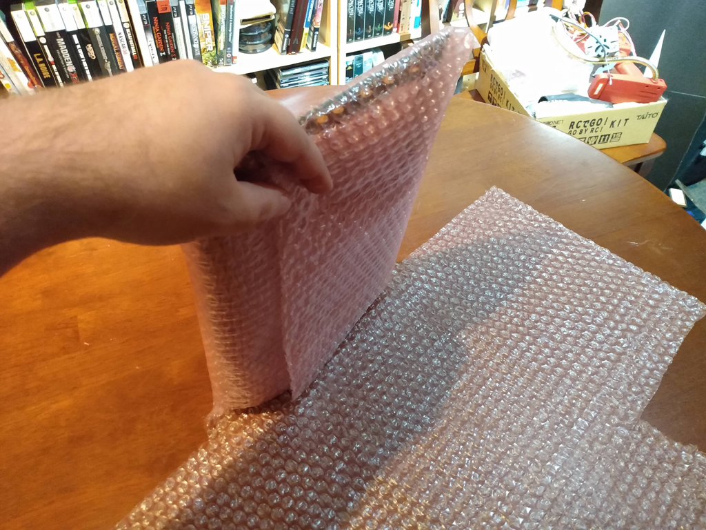
- Fold the wings over the bottom of the PCB, ensuring that they’re taught and flat and that the PCB’s bottom edge is well aligned with the bubble wrap.
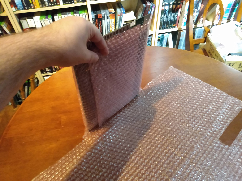
- Set the PCB down such that it is resting on the wings you just folded.
- Making sure everything is taught, flat, and aligned fold over the next set of wings
- making sure everything is taught, flat and aligned flip over the PCB again and then fold over the next set of wings. Repeat this until you’re left with just one flap.
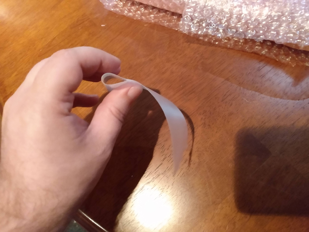
Step 5 -Tape
- You should now have a neatly wrapped PCB with just a single flap that needs to be taped. If you’ve got the Polyethylene cloth tape then you finish with a single piece parallel with the edge of the flap as shown below.
- ALTERNATIVELY if you’re using Clear Packing tape I’d recommend cutting off a piece and folding and flattening a loop on one end and then placing perpendicular to the flap edge, as shown below [Note: I used the Polyethylene cloth tape for these pictures so you can see what I’m doing as the clear packing tape didn’t show up in photos]
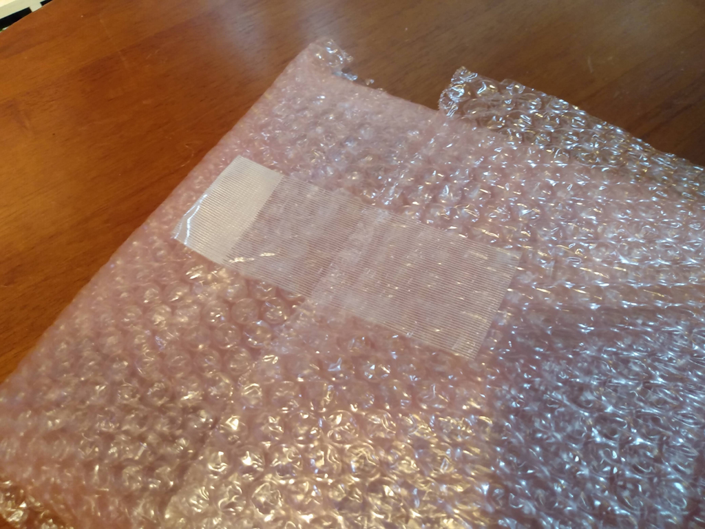
Step 6 – Label [Optional]
- Since it’s now harder to see what the PCB is you can finish it off with a label. I typically put the system or the manufacturer in parenthesis at the start of the label followed by the game name. But I’d encourage you to label in whatever organizational scheme makes sense to you.
- You can get fancy with designing and printing your own labels or simply cut a strip of paper and write it out with a marker.
- I recommend affixing the label over the bubble wrap that covers the JAMMA edge using a piece of clear packing tape that covers the entire label.
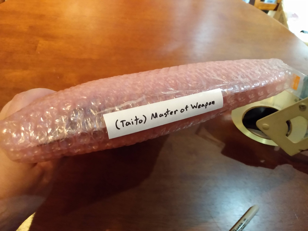
Placing the label in this position gives you a clear indication as to how the PCB is oriented inside of the bubble wrap. It also helps reinforce the area over the JAMMA edge and the fold of the bubble wrap that will be exercised most frequently.
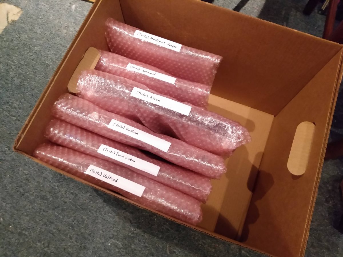
The Result
This method protects both faces and every edge of the PCB with multiple layers of bubble wrap. The cuts we made custom fit the bubble wrap to the specific PCB which allows it to stay quite compact while also maximizing protection. And the cuts also make it easy to re-wrap your PCB (just follow step 4 again).
Personally when I unwrap a PCB to play it I will often fold up the bubble wrap (again, following step 4) without the PCB in it and then put the wrap back where the PCB is normally stored as a place holder.
Storage
Where do you put all of your bubble wrapped PCBs, and how do you store them?
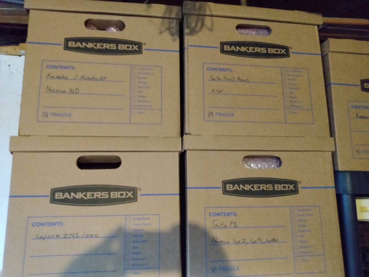
Personally I feel it’s best to store PCBs perpendicular to the ground. resting a PCB on it’s edge instead of it’s face is actually safest for PCBs of this size as it helps prevent sagging and warping. You definitely don’t want to stack PCB on top of one and other. and have the weight of the PCBs higher in the stack bearing down the PCBs lower in the stack. Similarly I’ve seen photos of long shelves in with many PCBs vertical but leaning on each other; this isn’t much better. What I propose is placing a small collection of PCBs vertically into a box to reduce the “leaning weight” and then place that box on a shelf somewhere.
I’ve seen people use plastic storage totes for this. I’m not a fan of this solution as they typically have rounded interior edges that really eat away at the usable volume for something like PCB storage, and they don’t have nice flat bottoms and walls for the PCBs to rest against. I’ve also seen these containers generate static, which is no good (even if we are using anti-static bubble wrap.) For these reasons I think a cardboard based box is better.
Another issue I’ve found is that most low-cost shelving units seem to have the same height, width and depth to their shelves, and sourcing boxes that work with that height width and depth is difficult. I’ve got a number of large plastic shelving units from HomeDepot and Lowes that I want to be able to maximize the shelf space on.
The Ideal solution I’ve found is the “Medium” sized “Bankers Box” brand Bankers’s Box.
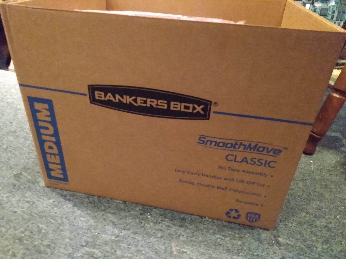
- No tape required, box folds into position
- has a lid that is easily removable instead of flaps that need to be taped or woven together
- has handles for easily lifting and moving
- this brand and size fits PERFECTLY with 2 boxes per shelf on most of the shelving units I own (your mileage may vary)
- even without a shelf boxes can also be stacked and the weight of the upper boxes rests on the lower boxes, rather than the PCBs inside of them.
Final Thoughts
So after years of collecting and trying dozes of different storage solutions, this is the one I finally settled on. I’ve been quite happy with it. Maybe this is the right solution for you? maybe not? maybe you want to use this method for shipping but not storage? maybe you want to use it for storage but not shipping? Maybe you want to develop your own technique based on this? Do what works for you! I just wanted to share the fruits of my research and give you my thoughts behind why I chose the solution I did.
Happy Collecting!
Good idea, I might have to give that a try. I just add feets to my pcbs and then screw them onto a cheap ikea cutting board then wrap them in an antistatic bag then slide that into a USPS box. Clearly it’s not very elegant solution.